Edgi-Talk_M33_S_HyperRam Example Project
中文 | English
Introduction
This example project is based on a Bare Metal architecture, mainly demonstrating and configuring Secure M33 HyperRam features. Additionally, this project can serve as a foundational template for secondary development or project creation, helping users quickly get started and extend functionality.
HyperRAM Overview
1. General Description
HyperRAM is a high-performance, low-pin-count (LPC) DRAM initially introduced by Cypress (now Infineon).
It uses the HyperBus interface, primarily targeting applications requiring high bandwidth, low power, and simple interfaces, such as embedded systems, display control, IoT devices, and automotive electronics.
HyperRAM is classified as pSRAM (Pseudo-SRAM): externally it behaves like SRAM (simple read/write without user refresh), but internally it is low-power DRAM (self-refresh).
2. Architecture and Interface
HyperRAM uses the HyperBus interface, characterized by:
Few pins: typically only 13 signal pins (8-bit data bus + control/clock), greatly reducing PCB complexity compared to traditional SDRAM (dozens of pins).
Double Data Rate (DDR) transfer: data is transmitted on both rising and falling clock edges to increase bandwidth.
Serial control protocol: accesses memory using command-address-data sequences, simplifying design.
Interface structure:
Data lines DQ[7:0]: 8-bit bidirectional data
RWDS (Read-Write Data Strobe): data synchronization signal
CLK: clock input
CS#: chip select
RESET#: reset
CKE: clock enable
3. Working Principle
HyperRAM is accessed via command + address + data:
Command Phase
The host sends a read/write command and target address.
Latency Phase
HyperRAM prepares its internal memory array (configurable latency).
Data Transfer Phase
Data is transferred on DQ[7:0] in DDR mode, with RWDS providing data synchronization.
Internally it uses DRAM technology with self-refresh, but externally it behaves like SRAM — users do not need to manage refresh operations.
4. Performance Features
Data bus width: 8-bit
Operating voltage: 1.8 V or 3.0 V (low-power design)
Data rate: up to 400 MB/s (200 MHz DDR × 8-bit)
Capacity range: 32 Mb ~ 512 Mb (4 MB ~ 64 MB)
Low power: supports deep sleep mode, standby current < 10 µA
Simple interface: high-speed access using only 13 pins
5. Advantages of HyperRAM
Low pin count
Significantly reduces pin requirements compared to traditional SDRAM/PSRAM (30+ pins), saving PCB routing.
High bandwidth
DDR interface, bandwidth up to 400 MB/s, suitable for image buffering and display refresh.
Low power consumption
Ideal for battery-powered devices such as IoT and wearable devices.
Ease of use
Behaves like SRAM externally, simple and user-friendly, no manual refresh needed.
6. Comparison with Other Memories
Feature |
HyperRAM |
SDRAM / DDR |
SRAM |
NOR Flash |
|---|---|---|---|---|
Interface |
HyperBus (13-pin) |
Parallel 16~32-bit |
Parallel/Serial |
SPI/QSPI |
Capacity |
32Mb ~ 512Mb |
64Mb ~ 1Gb+ |
Small (Kb~Mb) |
4Mb ~ 2Gb |
Bandwidth |
~400 MB/s |
~800 MB/s+ |
~50 MB/s |
~100 MB/s |
Power |
Low |
High |
Low |
Low |
Applications |
Cache/Frame Buffer |
System Memory |
High-speed small storage |
Program Storage |
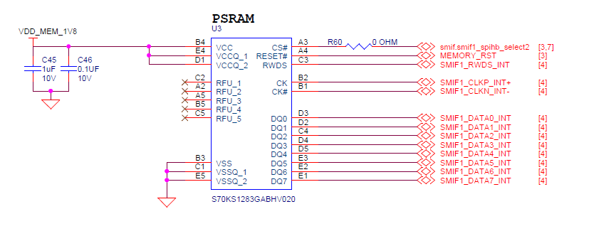
Hardware Description
HyperRam Interface
Software Description
The project is developed based on the Edgi-Talk platform.
The example covers:
Secure region configuration
Basic startup process demonstration
The project code structure is simple and clear, making it easy to understand and port.
Usage
Build and Download
Open the project and compile it.
Connect the board’s USB interface to the PC using the onboard debugger (DAP).
Use the programming tool to flash the compiled firmware to the board.
Running Result
After flashing, power on the board to run the example.
The system will start successfully and jump to the M33 core, indicating that the secure configuration is effective.
Notes
To modify the graphical configuration, open the configuration file using the following tool:
tools/device-configurator/device-configurator.exe
libs/TARGET_APP_KIT_PSE84_EVAL_EPC2/config/design.modus
After modification, save the configuration and regenerate the code.
Startup Sequence
The system starts in the following order:
+------------------+
|   Secure M33     |
|  (Secure Core)   |
+------------------+
          |
          v
+------------------+
|       M33        |
| (Non-Secure Core)|
+------------------+
          |
          v
+-------------------+
|       M55         |
| (Application Core)|
+-------------------+
⚠️ Please strictly follow the above flashing sequence; otherwise, the system may fail to run properly.